

The digital age, a period of unprecedented technological acceleration, is profoundly shaped by the ubiquitous devices that connect and empower us daily. Yet, at the core of every smartphone, every computer, and every integrated circuit lies a fundamental material, an unsung hero of innovation: silicon. This remarkable element, atomic number 14, has quietly shaped our modern world, transforming industries and laying the very groundwork for our collective future.
From its humble origins as the second most abundant element in Earth’s crust to its refined role in powering global communication networks, silicon’s journey is a testament to scientific discovery and relentless engineering. Its unique properties, once mysteries to early chemists, have been harnessed to create the sophisticated semiconductor technologies that are the bedrock of our information society. Without silicon, the interconnected and intelligent world we know would simply not exist.
This in-depth exploration will unveil the multifaceted importance of silicon, delving into its fundamental nature, its rich history, and the pivotal moments that transformed it. We’ll examine how this hard, brittle crystalline solid, with its distinctive bluish-grey metallic lustre, became the cornerstone of an entire era, offering practical insights into the very fabric of our technological landscape.
1. Chemical Element Fundamentals
Silicon is formally classified as a chemical element, distinguished by its symbol Si and an atomic number of 14. It manifests as a hard, brittle crystalline solid, characterized by a blue-grey metallic lustre. Often considered a metalloid, it holds a unique position with properties spanning both metallic and nonmetallic categories. Crucially, silicon is a semiconductor, a property underpinning its widespread technological significance. It resides in group 14 of the periodic table, below carbon and above germanium, tin, lead, and flerovium.
Beyond its industrial applications, silicon holds biological importance. It is a significant element essential for physiological and metabolic processes within plants. Moreover, certain marine organisms like sea sponges, diatoms, and radiolaria utilize silica—a compound of silicon and oxygen—to secrete intricate skeletal structures. This biological presence highlights silicon’s pervasive influence across natural systems.
Silicon is widely recognized as the predominant semiconductor material, a distinction earned through its versatile applications in electrical devices such as transistors, solar cells, and integrated circuits. Its suitability stems from favorable characteristics, including a significant band gap, an expansive optical transmission range, an extensive absorption spectrum, and its capacity for surface roughening and effective anti-reflection coating. These properties collectively make it indispensable for modern technology.
Read more about: Electricity Unveiled: A Consumer Guide to Its Fundamental Concepts, History, and Modern Applications

2. Abundance and Occurrence
Silicon ranks as the eighth most common element by mass in the universe. This cosmic prevalence, however, differs significantly within our own solar system and particularly on Earth, due to substantial elemental separation during formation. On Earth, silicon constitutes approximately 27.2% of the Earth’s crust by weight, making it the second most abundant element, after oxygen (45.5%).
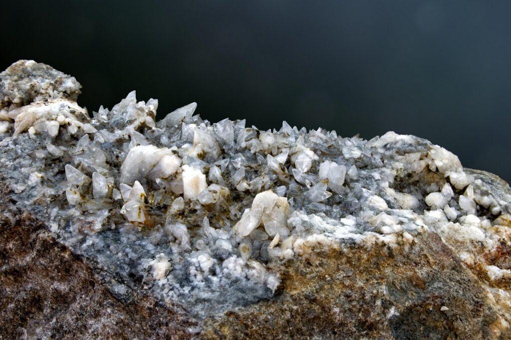
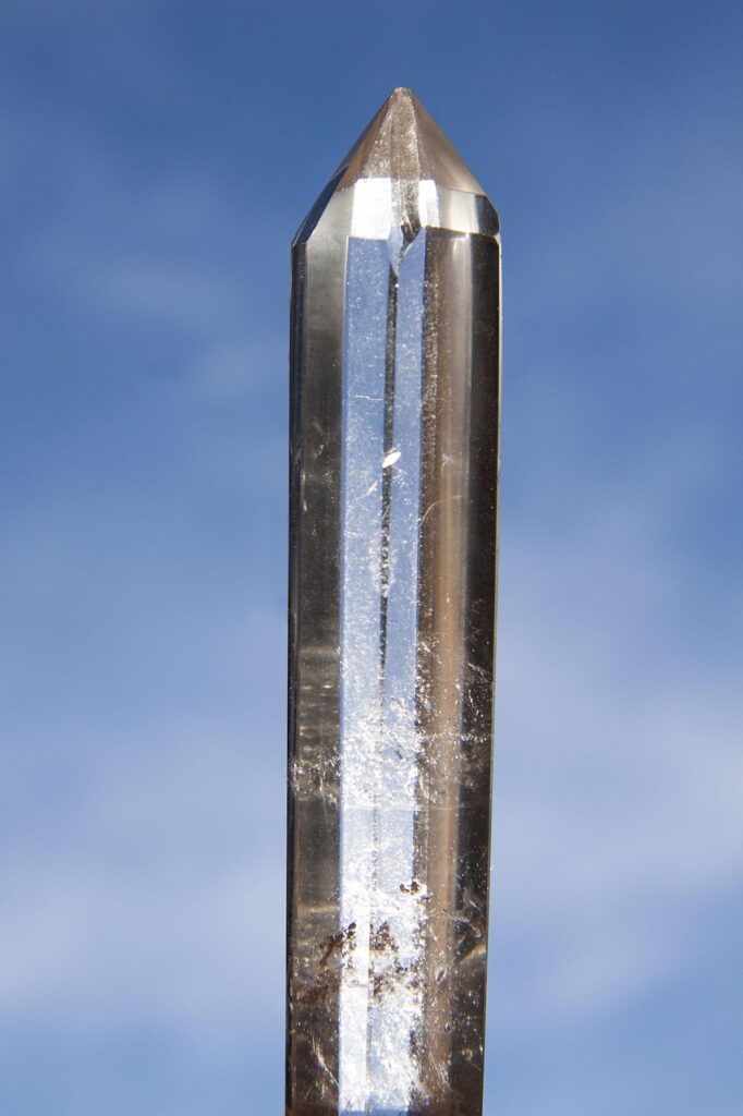
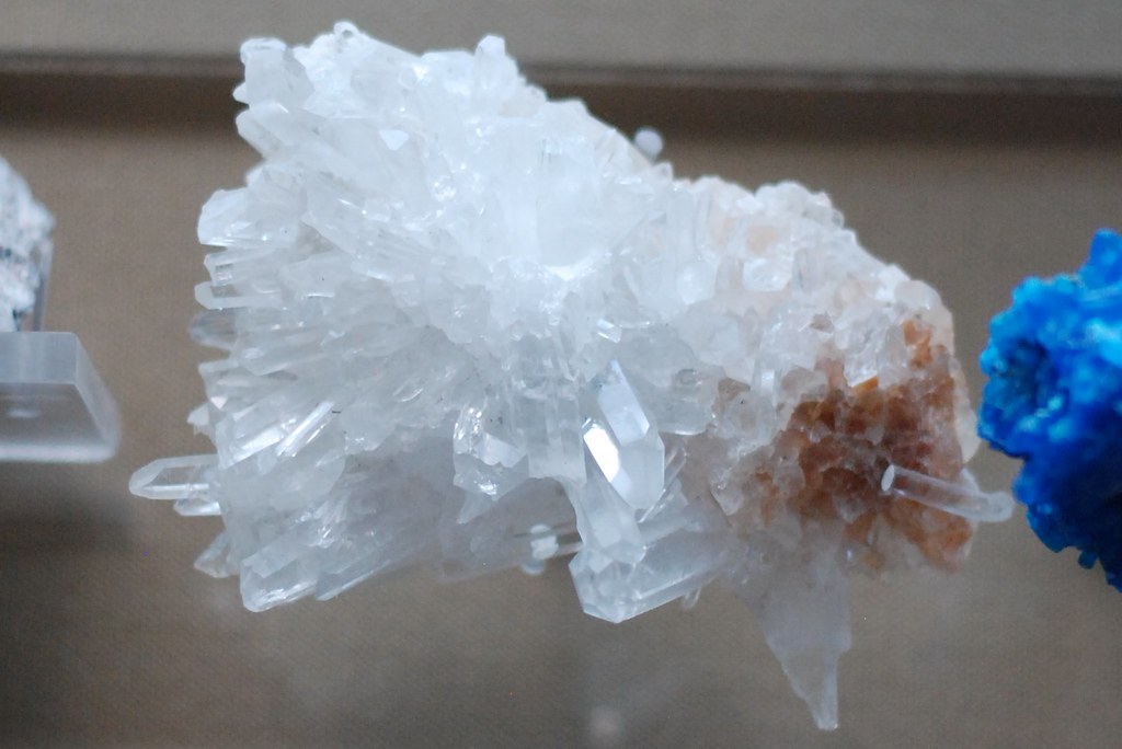
Silicon is almost always found associated with oxygen in nature, forming the foundation of countless minerals. Its pure elemental form is a rarity in the Earth’s crust, a testament to its high chemical affinity for oxygen. Over 90% of the Earth’s crust is composed of silicate minerals, clearly indicating its foundational role in planetary geology. These compounds are widely distributed across space, appearing in cosmic dusts, planetoids, and larger planetary bodies.
Further fractionation occurred during Earth’s formation through planetary differentiation. The mantle, comprising 68.1% of Earth’s mass, is predominantly composed of denser oxides and silicates, with olivine ((Mg,Fe)2SiO4) as an example. Lighter siliceous minerals such as aluminosilicates rose to the surface, forming the crust, where silicon’s impact on life and industry is most keenly felt.
Read more about: Mastering Midlife: 12 Key Foods for Men’s Strength and Unwavering Vitality After 40

3. Historical Discovery and Naming
The formal discovery of silicon spans decades of scientific inquiry. In 1787, Antoine Lavoisier suspected silica was an oxide of a fundamental element. However, silicon’s immense chemical affinity for oxygen prevented him from isolating the pure element. Later, in 1808, Sir Humphry Davy attempted isolation and proposed “silicium” from the Latin ‘silex, silicis’ (flint), believing it a metal. This name influenced many other languages.
An incomplete step occurred in 1811 when Gay-Lussac and Thénard likely prepared impure amorphous silicon by heating potassium metal with silicon tetrafluoride. Yet, they did not purify or identify it as a new element. The lasting name, “silicon,” was coined in 1817 by Scottish chemist Thomas Thomson. He retained part of Davy’s proposal but changed the suffix to “-on,” accurately believing silicon to be a nonmetal, similar to boron and carbon.
The definitive isolation came in 1824 when Jöns Jacob Berzelius successfully prepared amorphous silicon. Using a similar method to Gay-Lussac’s, he purified the product into a brown powder through repeated washing. This rigorous purification earned Berzelius credit for the element’s discovery. In the same year, Berzelius also became the first to prepare silicon tetrachloride, building on earlier work by Carl Wilhelm Scheele.
Read more about: Get Ready to Dive Deep: 15 Unforgettable Elements of Toni Morrison’s Pulitzer-Winning Novel ‘Beloved’
4. Key Physical Properties
Silicon possesses a unique suite of physical properties that make it exceptionally valuable for myriad applications. At standard conditions, it presents as a hard and brittle crystalline solid, characterized by a distinctive blue-grey metallic lustre, hinting at its semi-metallic nature and conductivity.
One of its most defining physical attributes is its high melting point of 1414 °C (1687 K) and boiling point of 3265 °C (3538 K). These figures are remarkably high, placing silicon with the second highest melting and boiling points among all metalloids and nonmetals, surpassed only by boron. Such extreme temperatures underscore the robust nature of bonds within its crystalline structure.
Structurally, silicon crystallizes in a diamond cubic crystal lattice, a giant covalent structure where silicon atoms form sp3 hybrid orbitals, dictating its tetrahedral coordination. This architecture contributes directly to its hardness and high melting point. Interestingly, upon melting, silicon contracts, as the long-range tetrahedral network of bonds breaks up and voids are filled in. Its density is 2.329085 g/cm³ at 20°C, and it exhibits a Mohs hardness of 6.5.
Read more about: Unlocking Peak Potential: 12 Cutting-Edge Wearable Technologies Powering Professional Teams to New Performance Heights

5. *lectrical Properties and Semiconductor Nature
At standard temperature and pressure, silicon is a shiny semiconductor with a bluish-grey metallic lustre, exhibiting resistivity that drops as temperature rises. This property stems from a small energy gap (band gap) between its valence and conduction bands. Pure silicon is effectively an insulator at room temperature, with the Fermi level halfway between these bands, requiring significant energy for electrons to conduct.
This insulating characteristic is precisely what makes silicon valuable through doping, which alters its electrical conductivity. Doping with pnictogen elements (e.g., phosphorus, arsenic) introduces extra electrons, creating an n-type semiconductor where electrons are primary charge carriers. Conversely, doping with group 13 elements (e.g., boron, aluminum) introduces acceptor levels that trap electrons, creating p-type semiconductors where positive “holes” are the primary charge carriers.
The marvel of silicon in electronics emerges with the p–n junction, formed by joining n-type and p-type silicon. This junction acts as a diode, rectifying alternating current by allowing current to pass more easily in one direction. An n–p–n junction, a thin layer of weakly p-type silicon between two n-type regions, forms the basis of a transistor. By biasing the emitter and collector, this transistor acts as a triode amplifier, enabling the amplification and switching functions vital for modern electronic circuits.
Read more about: The Nanotech Revolution: 15 Everyday Products Poised for Transformation Within Five Years

6. The Dawn of Silicon Semiconductors
Silicon’s preeminence in semiconductor technology was a gradual journey. Early semiconductor devices used galena, such as Ferdinand Braun’s crystal detector (1874) and Jagadish Chandra Bose’s radio crystal detector (1901), laying conceptual groundwork. The first specific application for silicon arrived in 1906 with American engineer Greenleaf Whittier Pickard’s silicon radio crystal detector.
A crucial breakthrough occurred in 1940 when Russell Ohl, at Bell Labs, discovered the p–n junction and photovoltaic effects within silicon, revealing its potential to convert light into electricity and control current. World War II demands accelerated research, leading to techniques in 1941 for producing high-purity germanium and silicon crystals for radar microwave detectors.
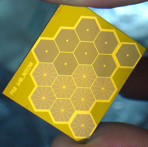
The mid-century saw rapid innovation. In 1947, William Shockley theorized a field-effect amplifier, leading to John Bardeen and Walter Brattain building the first working point-contact transistor (germanium). However, the focus shifted to silicon when Morris Tanenbaum fabricated the first silicon junction transistor at Bell Labs in 1954. Carl Frosch and Lincoln Derick’s accidental discovery in 1955 that silicon dioxide could be grown on silicon led to the first planar transistors in 1957. Building on this, Robert Noyce developed the first silicon-based integrated circuit in 1959, integrating multiple transistors onto a single chip and initiating the microchip revolution.

7. The Silicon Age
The late 20th to early 21st century is aptly christened the “Silicon Age,” capturing elemental silicon’s profound impact on our modern world economy. Also known as the Digital or Information Age, it’s named for silicon’s role as the dominant material in electronics and information technology, much like previous ages were defined by their key materials.
Central to this era’s technological explosion is the Metal-Oxide-Semiconductor Field-Effect Transistor (MOSFET), also known as the MOS transistor. This key component enables the miniaturization and efficiency of modern electronics, tracing its lineage to the first silicon semiconductor oxide planar transistor innovated by Frosch and Derick in 1957.
While most commercially produced silicon serves industrial construction or metallurgical alloys, the small, highly purified portion (less than 15% of total) is crucial to the Silicon Age. This meticulously refined silicon is the core material for transistors and integrated circuit chips in nearly every modern device, from smartphones to supercomputers, making its unparalleled purity and semiconductor properties indispensable.
The economic implications are immense. In 2019, 32.4% of the semiconductor market segment was for networks and communications devices, showing silicon’s foundational role. The semiconductor industry is projected to reach $726.73 billion by 2027, testifying to ongoing innovation. So pervasive is silicon’s influence that its name labels numerous tech regions globally, including the iconic “Silicon Valley” in California, and others like “Silicon Wadi” in Israel, “Silicon Forest” in Oregon, and “Dubai Silicon Oasis” in Dubai, reflecting its pivotal role in technological advancement and economic dynamism.
Read more about: The Billion-Dollar Ballgame: Unveiling Forbes’ 15 Most Valuable Sports Franchises and What Drives Their Astronomical Worth

8. Isotopic Distinctions
Naturally occurring silicon is a fascinating blend of three stable isotopes: 28Si, 29Si, and 30Si. The vast majority, about 92.24%, is 28Si, while 29Si makes up 4.67% and 30Si accounts for 3.07%. This natural distribution offers a unique isotopic signature for the element, crucial for understanding its prevalence and behavior.
Among these stable isotopes, 29Si holds a special place in scientific analysis due to its nuclear spin (I = 1/2), making it particularly useful in advanced analytical techniques such as Nuclear Magnetic Resonance (NMR) and Electron Paramagnetic Resonance (EPR) spectroscopy. These methods allow scientists to probe the intricate structures and dynamics of silicon-containing materials at a molecular level, unlocking deeper insights.
Beyond its stable forms, silicon also has twenty-two characterized radioisotopes. The stablest of these are 32Si, with a half-life of approximately 157 years, and 31Si, which has a half-life of 2.62 hours. These radioisotopes offer pathways for scientific research, with 31Si being useful for quantitative analysis through its characteristic beta decay to stable 31P.
The cosmic origins of these isotopes are equally compelling. All three stable silicon isotopes are produced in Type Ia supernovae through the oxygen-burning process, with 28Si forming as part of the alpha process, explaining its high abundance. The fusion of 28Si with alpha particles by photodisintegration rearrangement in stars is even known as the silicon-burning process, a critical stage in stellar nucleosynthesis preceding a star’s violent collapse and explosion.
Isotopic variations of silicon are also significant in Earth’s biogeochemical cycles, particularly in oceans. Different fluxes, such as groundwater and riverine transport, carry distinct isotopic compositions of silicon, contributing to measurable variations in oceanic 30Si values. This deep water 30Si gradient, especially between the Atlantic and Pacific oceans, is often associated with oceanic productivity, offering clues to marine ecosystems and global climate patterns.
9. Unique Chemical Behavior
Crystalline bulk silicon exhibits a rather inert nature under standard conditions, a trait that shifts dramatically at elevated temperatures. A key factor in its stability is the formation of a thin, continuous surface layer of silicon dioxide (SiO2), which acts as a protective shield against oxidation, similar to aluminum. This layer effectively prevents significant reaction with the air below 900 °C.
However, this protective layer has its limits. Between 950 °C and 1160 °C, the rate of vitreous dioxide formation rapidly increases. At even higher temperatures, around 1400 °C, atmospheric nitrogen begins to react, forming silicon nitrides like SiN and Si3N4. Silicon also shows reactivity with other nonmetals, engaging with gaseous sulfur at 600 °C and gaseous phosphorus at 1000 °C.
Despite its inertness to most aqueous acids, silicon readily succumbs to halogens. Fluorine, for instance, vigorously attacks silicon at room temperature. Chlorine requires about 300 °C to react, while bromine and iodine need around 500 °C. Furthermore, silicon is oxidized and complexed by hydrofluoric acid mixtures containing chlorine or nitric acid, leading to the formation of hexafluorosilicates. It also conveniently dissolves in hot aqueous alkali, forming silicates.
Molten silicon presents a stark contrast, becoming exceptionally reactive. It readily alloys with most metals to form silicides and is powerful enough to reduce most metal oxides, a testament to the high heat of formation of silicon dioxide. This extreme reactivity means molten silicon challenges virtually every known crucible material, except its own oxide, SiO2, due to its strong binding forces for light elements and high dissolving power.
Comparing silicon to its lighter congener carbon, fundamental differences emerge, despite both forming tetrahedral derivatives. Silicon’s 3p subshell is more diffuse, leading to less effective hybridization with its 3s subshell and a lower electronegativity (1.90 vs. carbon’s 2.55). This results in a much weaker tendency for catenation (Si-Si bonds vs. C-C bonds) and generally less stable multiply bonded silicon compounds, a clear departure from carbon’s rich organic chemistry.
Read more about: Unlocking Peak Potential: 12 Cutting-Edge Wearable Technologies Powering Professional Teams to New Performance Heights
10. Advanced Production Methods
The journey of silicon from its natural state to industrial utility involves sophisticated production processes tailored to achieve varying levels of purity. For applications not requiring ultra-high purity, silicon with 96–99% purity is typically produced through the carbothermal reduction of quartzite or sand. This process takes place in an electric arc furnace, where an excess of SiO2 is maintained to prevent the undesirable accumulation of silicon carbide (SiC).
A significant portion of elemental silicon production, approximately 80% globally, comes in the form of ferrosilicon, an iron-silicon alloy. This is primarily created by conducting the carbothermal reduction in the presence of scrap iron, ensuring low amounts of phosphorus and sulfur. China leads the world in elemental silicon supply, largely through ferrosilicon, which is crucial for the iron and steel industry, serving as an alloying addition and de-oxidizer.
Achieving the extreme purity demanded by semiconductor applications requires even more advanced methods. This hyper-pure silicon, where impurity levels must be less than 1 part per 10^10, or even 1 part per 10^12 in specialized cases, is derived from the reduction of tetrachlorosilane (silicon tetrachloride) or trichlorosilane. These volatile compounds are first purified through repeated fractional distillation, a highly effective separation technique.
Following distillation, these purified compounds are reduced to elemental silicon, often using very pure zinc metal as the reducing agent. The resulting spongy silicon pieces are then melted and meticulously grown into cylindrical single crystals, which are further refined through a process known as zone refining. This multi-step purification ensures the unparalleled quality needed for advanced electronics.
Beyond traditional methods, silicon nanostructures can now be directly produced from silica sand. These advanced materials are synthesized using conventional metalothermic processes or through combustion synthesis. Such nanostructured silicon holds immense promise for various functional applications, including anodes for lithium-ion batteries, future computing devices like memristors, and photocatalytic applications, driving forward the next wave of technological innovation.
Read more about: The Definitive Guide to Joint Health: 13 Expert-Recommended Supplements for Pain Relief and Mobility

11. Commercial Uses: Structural Compounds
The vast majority of silicon’s commercial utility stems from its unpurified forms, often requiring minimal processing from natural minerals. Over 90% of the Earth’s crust is composed of silicate minerals, which are compounds of silicon and oxygen, frequently integrated with metallic ions. These fundamental building blocks of our planet directly translate into numerous indispensable commercial applications.
Many of these natural silicon compounds serve as crucial structural materials. Common examples include clays, silica sand, and various types of building stone, which have been utilized by civilizations for millennia. Their inherent strength and abundance make them foundational elements in construction and infrastructure development globally.
Silicates are central to modern construction, forming the basis of Portland cement. This cement, predominantly composed of calcium silicates, is essential for creating mortar and modern stucco. More critically, when combined with silica sand and gravel—which itself often contains silicate minerals like granite—it forms concrete, the robust material underpinning the largest industrial building projects of the contemporary world, from roads to towering structures.
Furthermore, silicon dioxide, or silica, is a key ingredient in specialized ceramics like fire brick, valued for its heat resistance. Silicate minerals are also integral to whiteware ceramics, a broad class of products typically made from fired clay minerals such as kaolinite-based porcelain, showcasing silicon’s versatility in crafting durable and aesthetically pleasing goods.
Traditional glass, primarily silica-based soda-lime glass, represents another pervasive application, providing transparent windows and reliable containers for countless purposes. Beyond this, advanced silica-based glass fibers are engineered for optical fiber communications, enabling high-speed data transmission, and are also employed in fiberglass for structural reinforcement and glass wool for efficient thermal insulation, demonstrating silicon’s critical role in both everyday items and cutting-edge technology.

12. Commercial Uses: Industrial Alloys
Elemental silicon, particularly in its metallurgical grade form, plays a vital role in enhancing the properties of various metal alloys, extending its influence beyond the realm of pure electronics. A significant application is its addition to molten cast iron, often as ferrosilicon or silicocalcium alloys, to markedly improve casting performance for thin sections and to inhibit the formation of cementite when exposed to air.
In the steel industry, the presence of elemental silicon in molten iron acts as a crucial deoxidizer. This function is paramount for closely controlling the steel’s carbon content, which must be precisely maintained within narrow limits for each specific type of steel. This makes ferrosilicon production and consumption a direct indicator of the health and output of the global steel industry.
While grossly impure, this form of elemental silicon accounts for a massive 80% of the world’s total use of free silicon. Beyond its deoxidizing role, silicon is also a critical component in transformer steel, where it significantly modifies the material’s resistivity and improves its ferromagnetic properties, enhancing the efficiency and performance of electrical transformers.
The properties of silicon are also leveraged to modify alloys with non-iron metals. Approximately 55% of the world’s metallurgical purity silicon is dedicated to producing aluminum-silicon alloys, known as silumin alloys. These are predominantly used in aluminum part casts, with the automotive industry being a major consumer due to their superior casting characteristics.
Silicon’s importance in aluminum casting lies in its ability to form a eutectic mixture with aluminum when present in a sufficiently high amount (around 12%). This mixture solidifies with very minimal thermal contraction, a property that drastically reduces the formation of tears and cracks caused by stress as the casting alloys cool. Furthermore, silicon substantially boosts the hardness and wear-resistance of aluminum, making these alloys invaluable for robust applications.

13. Advanced Crystal Structures and Allotropes
Silicon’s inherent versatility extends to its fascinating crystal structures, providing deep insights into its physical and atomic behavior. Under standard conditions, silicon crystallizes in a giant covalent structure, specifically a diamond cubic crystal lattice. This structure is formed through sp3 hybrid orbitals, which dictate its tetrahedral coordination and contribute directly to its notable hardness and high melting point of 1414 °C, requiring substantial energy to break the robust covalent bonds.
A peculiar characteristic of silicon is its behavior upon melting; unlike most substances, silicon contracts. This intriguing phenomenon occurs because the long-range tetrahedral network of bonds breaks down, allowing voids within that network to be filled. This is analogous to water ice, which also contracts when its hydrogen bonds are disrupted during melting.
While the standard diamond cubic structure (Si-I) is thermodynamically stable at standard pressure, silicon reveals a more complex nature under extreme conditions. Several other crystal structures, or allotropes, are known to form at higher pressures. The general trend observed is an increase in coordination number as pressure intensifies, leading to diverse structural modifications.
This evolution culminates in a hexagonal close-packed allotrope known as Si–VII, which forms at pressures around 40 gigapascals. Another notable allotrope is BC8 (or bc8), characterized by a body-centred cubic lattice with eight atoms per primitive unit cell. This form can be created under high pressure and remains metastable even at lower pressures, showcasing silicon’s ability to adopt exotic structural arrangements.
Further pushing the boundaries of material science, it has become possible to construct silicene layers. These two-dimensional structures are analogous to graphene, the celebrated carbon allotrope, suggesting potential for revolutionary applications in nanoelectronics. The continuous exploration of silicon’s crystal structures and allotropes underscores its profound significance in materials science and its ongoing potential for innovative technological advancements.
Read more about: The Enduring Significance of Four: An In-depth Analysis of Its Pervasive Influence Across Disciplines
From the cosmic forge to the intricate microchips that power our digital lives, silicon’s story is one of fundamental importance and relentless innovation. This remarkable element, once a mere suspect in Lavoisier’s laboratory, has transformed into the bedrock of modern technology, enabling everything from the concrete foundations of our cities to the complex computations within our smart devices. Its unique properties, from its isotopic signatures to its diverse crystal structures and versatile chemical behavior, continue to fascinate scientists and engineers alike. As we look to the future, silicon, in its various forms—from robust structural materials to ultra-pure semiconductors and novel nanostructures—will undoubtedly remain an indispensable force, shaping new frontiers in computing, energy, and materials science, ensuring its enduring legacy as the true unsung hero of the modern world.


